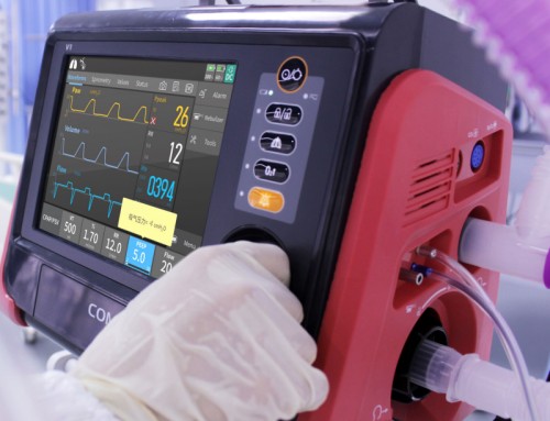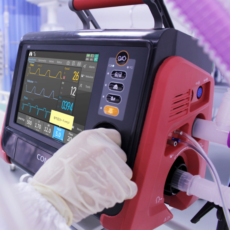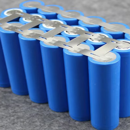
A clinical engineer conducts a rapid diagnostic scan using a handheld X-ray device in a busy hospital ward. When the trigger is pulled to initiate an exposure, the system demands an instantaneous 4.0A current burst. Even though the battery indicator shows ample remaining capacity, high cumulative internal resistance ($R_{\text{DC}}$) across the 18650 series cell stack produces an immediate voltage drop. The terminal voltage dips below the DC-DC converter’s minimum input threshold, triggering a brownout reset that interrupts image acquisition and delays patient care. Minimizing internal impedance across multi-series 18650 battery packs is a core engineering requirement to eliminate voltage sag, prevent parasitic $I^2R$ resistive heating, and maintain predictable power delivery in portable medical and industrial equipment.
Cell-Level Selection and Precision Impedance Matching
Reducing total pack resistance begins at the cell selection stage before any physical welding or assembly takes place. In a multi-series array—such as a 3S1P configuration delivering a nominal 10.8V—the total equivalent series resistance equals the sum of individual cell resistances plus the resistance of physical interconnects and protection electronics.
Distinguishing AC (1 kHz) and DC Internal Resistance
Engineers must evaluate both $1\text{ kHz}$ AC internal resistance ($R_{\text{AC}}$) and true DC internal resistance ($R_{\text{DC}}$). $R_{\text{AC}}$ reflects the ohmic resistance of the electrolyte, separator, and current collectors under a low-amplitude AC signal. In contrast, $R_{\text{DC}}$ accounts for charge-transfer polarization and ion diffusion kinetics under active DC load currents. Premium Panasonic 18650 cells engineered for high energy density and stability provide low baseline impedance, allowing fully assembled 3S1P smart battery packs to achieve an overall internal resistance rating of $<150\text{ m}\Omega$ at $1\text{ kHz}$ ($25^\circ\text{C}$).
Cell Grading and Delta-Resistance Tolerance Bands
Combining cells with mismatched internal resistance in a series string creates electrical imbalance. Under a 4.0A load, cells with higher resistance experience greater voltage drop and localized $I^2R$ heating. This causes high-impedance cells to hit lower voltage limits prematurely during discharge, reducing usable pack capacity. Incoming Quality Control (IQC) protocols enforce strict cell grading, sorting 18650 cells into tight resistance bands ($\Delta R_{\text{AC}} \le 2\text{ m}\Omega$). Matching cell impedance ensures uniform voltage distribution across the 10.8V stack and prevents localized thermal stress.
Interconnect Metallurgy, Welding Geometry, and Busbars
Physical connections between 18650 cells contribute significantly to overall pack resistance. Selecting low-resistivity conductor materials and optimizing weld topology eliminates electrical bottlenecks along the primary current path.
Copper-Nickel Composites vs. Pure Nickel Strips
Standard battery assembly often uses pure nickel strips due to their spot-welding ease. However, pure nickel exhibits relatively high resistivity ($6.84 \times 10^{-8}\ \Omega\cdot\text{m}$), introducing parasitic resistance under high continuous loads. Replacing pure nickel with nickel-plated copper composite busbars or pure copper strips dramatically decreases interconnect resistance, as copper’s resistivity ($1.68 \times 10^{-8}\ \Omega\cdot\text{m}$) is roughly four times lower. For compact handheld diagnostic tools, using wide, thick busbars (e.g., $0.15\text{ mm to }0.20\text{ mm}$) expands the conductor cross-section, suppressing voltage drops across series junctions.
Spot Welding Parameters and Joint Contact Resistance
The mechanical interface between the busbar and the 18650 cell terminal represents a contact resistance point. Inadequate weld pressure or insufficient energy pulses leave micro-voids that elevate local resistance. Implementing precision micro-resistance spot welding or laser welding creates solid-state metallurgical bonds, maintaining individual joint resistance below $0.1\text{ m}\Omega$. Using slotted 4-point or 6-point weld patterns distributes current density evenly across the terminal surface, preventing localized hot spots during 2.41A charging or 4.0A discharging cycles.
| Engineering Parameter | Technical Value (Low-Impedance 3S1P Architecture) | System Integration Impact |
| Series-Parallel Topology |
3S1P (Panasonic 18650 Cells)
|
High energy density and low baseline cell impedance
|
| Nominal Voltage / Energy |
10.8V / 35.64Wh
|
Direct alignment with medical DC-DC input converters
|
| Rated Capacity (Nominal) |
3300mAh (3450mAh)
|
High capacity supporting extended clinical diagnostic cycles
|
| Max Charge Voltage / Current |
12.6V / 2.41A
|
Controlled JEITA-based thermal charge parameters
|
| Max Discharge Current |
4.0A
|
Sustains high-current diagnostic bursts without trip-outs
|
| Pack Internal Resistance |
<150mΩ @ 1kHz at 25°C
|
Suppresses voltage sag and $I^2R$ thermal dissipation
|
| Dimensions & Weight |
84.6mm × 58.5mm × 22.0mm | 180g ± 10g
|
Compact, ergonomic handle integration for handheld tools
|
| Physical Interface |
5-pin blade metal connector
|
Low contact resistance and secure mechanical retention
|
| Compliance Matrix |
CE / FCC / IEC 62133 / UN38.3 / PSE / UKCA
|
Pre-certified platform streamlining global regulatory access
|
BMS Layout Optimization, Switching MOSFETs, and Terminals
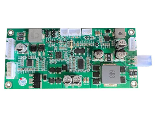
The Battery Management System (BMS) PCB introduces series components—such as protection MOSFETs, trace runs, sense resistors, and physical connectors—that add to overall pack impedance.
Parallel Low $R_{\text{DS(on)}}$ Power MOSFETs and Heavy Copper PCBs
Protection circuitry must prioritize low-loss switching components. Charge and discharge protection MOSFETs should be selected with sub-milliohm $R_{\text{DS(on)}}$ ratings ($<2\text{ m}\Omega$ per FET). Utilizing multi-layer PCBs with heavy copper plating ($2\text{ oz}$ to $4\text{ oz}$ copper weight) for high-current power paths minimizes resistive voltage drops between the cell stack and output terminals.
Contact Resistance at 5-Pin Blade Metal Interfaces
The physical interface connecting the battery pack to the host instrument represents a key contact resistance boundary. Utilizing a 5-pin blade metal connector with gold or silver plating ensures high contact force and resistance against surface oxidation. This secure mechanical engagement maintains low contact resistance and stable electrical contact during physical vibration or repeated insertion cycles in clinical settings.
Thermal Management, SMBus Telemetry, and Lifecycle Resistance Decay
Internal resistance is not static; it increases dynamically over the battery’s operational lifespan due to Solid Electrolyte Interphase (SEI) layer growth, electrolyte degradation, and thermal stress.
Preventing Thermal Gradients Across Series Strings
Temperature strongly affects lithium-ion impedance. Operating at lower temperatures increases electrolyte viscosity and charge-transfer resistance. Conversely, uneven heat dissipation within a compact 84.6mm × 58.5mm × 22.0mm enclosure causes inner cells to run hotter than outer cells. Hotter cells age faster, causing localized impedance growth. Symmetrical structural design and heat dissipation channels maintain uniform cell temperatures within specified operating windows ($0^\circ\text{C to }50^\circ\text{C}$ charge; $-20^\circ\text{C to }60^\circ\text{C}$ discharge).
Dynamic Resistance Tracking via SMBus v1.1 Protocols
As 18650 packs undergo cycling, integrated smart fuel gauges communicating via SMBus v1.1 continuously track changes in internal cell impedance. Advanced fuel gauge algorithms update cell resistance models dynamically, adjusting runtime calculations to prevent premature low-battery alarms. Integrated cell balancing and JEITA-based charge management further mitigate non-uniform aging, allowing high-quality 3S1P packs to retain at least 80% of their 3300mAh capacity after 500 complete charge-discharge cycles while maintaining stable internal impedance profiles.
For engineering teams developing portable medical and industrial equipment, selecting low-impedance, pre-certified power modules eliminates early voltage sag issues under load. Explore technical documentation and performance profiles for our fully integrated standard battery packs to streamline your system’s power design.
Frequently Asked Questions (FAQ)
1. How does high internal resistance affect handheld medical equipment performance?
High internal resistance leads to instantaneous $I \cdot R$ voltage drops under pulse loads. This voltage sag can cause the device’s internal power management circuits to sense a false under-voltage state, triggering premature resets or shutdowns even when the battery has ample remaining energy.
2. What is the difference between AC internal resistance ($R_{\text{AC}}$) and DC internal resistance ($R_{\text{DC}}$)?
$R_{\text{AC}}$ is measured at $1\text{ kHz}$ to evaluate ohmic resistance across the electrolyte and terminals. $R_{\text{DC}}$ measures true resistance during active current flow, incorporating charge-transfer and diffusion polarization effects. $R_{\text{DC}}$ is always higher than $R_{\text{AC}}$ and directly influences real-world runtime performance under load.
3. Why is copper preferred over pure nickel for interconnecting 18650 cells?
Copper has roughly four times the electrical conductivity of pure nickel ($1.68 \times 10^{-8}\ \Omega\cdot\text{m}$ vs $6.84 \times 10^{-8}\ \Omega\cdot\text{m}$). Using copper or copper-nickel composite busbars significantly decreases interconnect resistance and $I^2R$ heat generation across multi-series cell strings.
4. How does cell balancing help control pack internal resistance over time?
Integrated cell balancing prevents individual cells in a multi-series string from experiencing localized overcharge or deep discharge. By maintaining uniform voltage and state-of-charge across all series elements, cell balancing slows down uneven SEI layer growth and limits impedance growth over 500+ cycles.
5. What internal resistance value should engineers expect from a quality 3S1P smart 18650 battery pack?
A high-quality 3S1P smart 18650 pack utilizing Panasonic cells and optimized BMS circuitry typically maintains a total internal resistance of less than $150\text{ m}\Omega$ at $1\text{ kHz}$ ($25^\circ\text{C}$), ensuring stable voltage output under continuous loads up to 4.0A.