Strategies to Decrease Internal Resistance in Multi-Series 18650 Packs
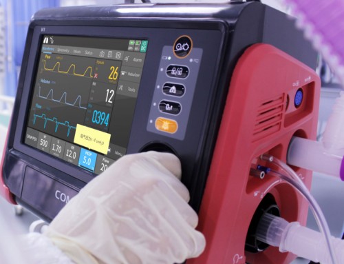
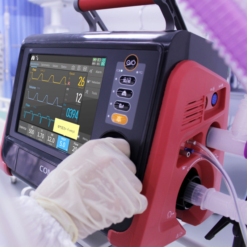
A portable surgical monitor draws an instantaneous 4.0A current surge as a motorized pump engages during a critical procedure. While the battery’s nominal state-of-charge reads 75%, the cumulative internal resistance ($R_{\text{DC}}$) across the multi-series cell array produces an immediate $I \cdot R$ voltage drop. The terminal voltage plummets below the power management IC’s lower threshold, forcing an abrupt system shutdown despite substantial remaining capacity. High internal resistance in multi-series 18650 lithium-ion packs not only induces voltage sag under transient loads but also converts valuable energy into parasitic $I^2R$ heat, accelerating thermal degradation and compromising device reliability. Minimizing internal resistance across multi-series 18650 configurations requires meticulous cell-level sorting, optimized interconnect metallurgy, low-impedance BMS routing, and thermal balancing.
Cell-Level Selection and Precision Impedance Sorting
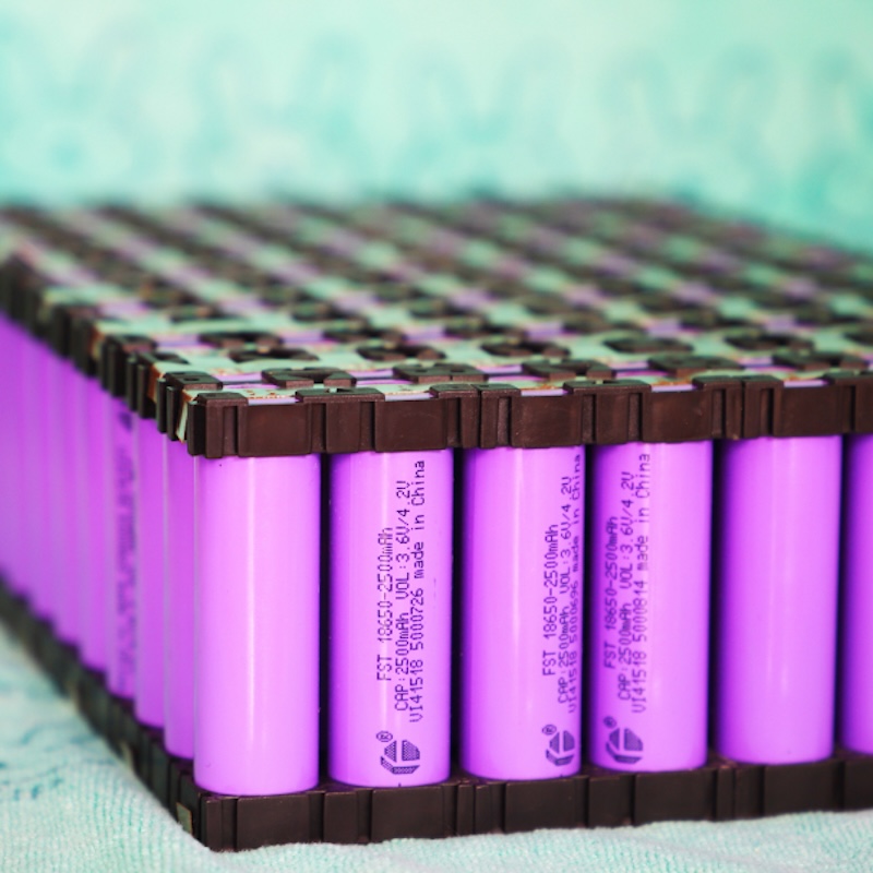
Reducing total pack resistance begins at the fundamental cell level before any physical assembly or spot welding occurs. In a multi-series array (such as a 3S1P configuration), total equivalent series resistance equals the cumulative sum of individual cell resistances plus internal interconnects.
AC vs. DC Internal Resistance Measurement Protocols
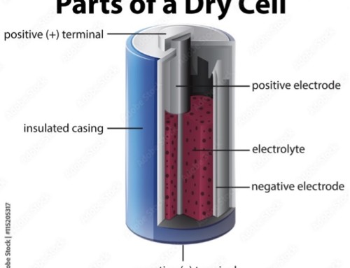
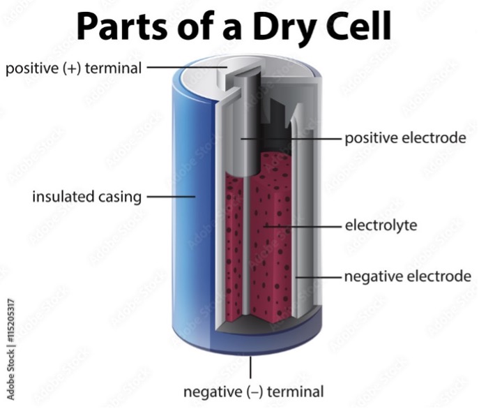
Engineers must distinguish between $1\text{ kHz}$ AC internal resistance ($R_{\text{AC}}$) and true DC internal resistance ($R_{\text{DC}}$). While $R_{\text{AC}}$ measures ohmic resistance across the electrolyte and separator using a $1\text{ kHz}$ sinusoidal signal, $R_{\text{DC}}$ captures charge-transfer polarization and mass-transport resistance under actual load conditions. Premium Panasonic 18650 cells selected for medical and precision instruments exhibit low baseline impedance, enabling fully assembled 3S1P smart packs to achieve an overall internal resistance rating of $<150\text{ m}\Omega$ at $1\text{ kHz}$ ($25^\circ\text{C}$).
Cell Matching and Delta-Resistance Thresholds
Pairing cells with mismatched internal resistance in a series string accelerates pack failure. High-IR cells experience greater $I^2R$ heating and steeper voltage drops during discharge, causing them to reach low-voltage cutoff thresholds prematurely. IQC protocols enforce strict cell grading, sorting incoming 18650 cells into narrow resistance bands ($\Delta R_{\text{AC}} \le 2\text{ m}\Omega$). Matching cells ensures equalized voltage distribution across the $10.8\text{V}$ nominal stack, preventing premature BMS cutoffs under load.
Interconnect Materials, Welding Geometry, and Busbar Optimization
Physical inter-cell connections contribute significantly to parasitic pack resistance. Selecting appropriate conductor materials and optimizing weld joint topology minimizes electrical bottlenecks between series groups.
Pure Nickel vs. Copper-Nickel Composite Busbars
Traditional battery assembly relies on pure nickel strips due to their ease of spot welding. However, pure nickel exhibits a resistivity of approximately $6.84 \times 10^{-8}\ \Omega\cdot\text{m}$, creating measurable resistance across high-current paths. Replacing standard nickel strips with nickel-plated copper composite busbars or pure copper strips drastically reduces interconnect resistance, as copper’s resistivity ($1.68 \times 10^{-8}\ \Omega\cdot\text{m}$) is roughly four times lower. For compact handheld instruments, utilizing wide, thick busbars (e.g., $0.15\text{ mm to }0.20\text{ mm}$ thickness) expands the cross-sectional conduction area, suppressing voltage drop across series junctions.
Spot Welding Parameters and Joint Resistance
The mechanical and electrical interface between the busbar and the 18650 cell terminal introduces contact resistance. Inadequate weld pressure or insufficient energy pulses result in high-resistance micro-voids. Implementing precision micro-resistance spot welding or laser welding creates solid-state metallurgical bonds, keeping individual joint resistance below $0.1\text{ m}\Omega$. Increasing the number of weld nuggets per terminal (e.g., 4-point or slotted 6-point weld patterns) distributes current density evenly and prevents localized heating.
BMS Circuit Topology, MOSFET Selection, and Terminal Connections
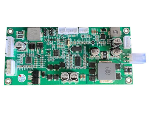
The Battery Management System (BMS) PCB introduces series components—including protection MOSFETs, trace runs, sense resistors, and physical connectors—that add to overall pack impedance.
Low $R_{\text{DS(on)}}$ Switching Matrices and Heavy Copper PCBs
Protection circuit design must prioritize low-loss components. Charge and discharge protection MOSFETs should be selected with sub-milliohm $R_{\text{DS(on)}}$ ratings ($<2\text{ m}\Omega$ per FET). Utilizing multi-layer PCBs with heavy copper plating ($2\text{ oz}$ to $4\text{ oz}$ copper weight) for high-current power paths minimizes resistive voltage drops between the cell stack and output terminals.
High-Reliability Blade Connectors and Contact Resistance
The physical interface between the battery pack and the host instrument represents a primary contact resistance point. Utilizing 5-pin blade metal connectors with gold or silver plating provides high contact force and resistance against oxidation. This secure mechanical engagement ensures stable electrical contact during physical shock and continuous device operation.
| Resistance Contributor | Impact on Total Pack IR | Mitigation Strategy | Engineering Target / Spec |
| Cell Ohmic & Electrochemical IR | High ($60\%\text{–}70\%$) | Precision IQC sorting of Tier-1 Panasonic 18650 cells | Mismatched $\Delta R_{\text{AC}} \le 2\text{ m}\Omega$; Pack IR $<150\text{ m}\Omega$ |
| Interconnect Busbars | Medium ($10\%\text{–}15\%$) | Copper-nickel composite or pure copper busbars | Expanded cross-section ($0.15\text{–}0.20\text{ mm}$) |
| Weld Joints | Low-Medium ($5\%\text{–}10\%$) | Laser or 4/6-point micro-spot welding | Joint contact resistance $<0.1\text{ m}\Omega$ per terminal |
| BMS Protection MOSFETs | Medium ($10\%\text{–}15\%$) | Parallel ultra-low $R_{\text{DS(on)}}$ power MOSFETs | $R_{\text{DS(on)}} < 2\text{ m}\Omega$ per switching element |
| PCB Power Traces | Low ($3\%\text{–}5\%$) | Multi-layer heavy copper trace layout | $2\text{ oz}$ to $4\text{ oz}$ copper trace weight |
| Output Terminals | Low ($2\%\text{–}5\%$) | Gold/silver-plated blade contacts | 5-pin blade connector interface |
Thermal Uniformity and Cycle-Life Resistance Mitigation
Internal resistance is not a static parameter; it increases dynamically over the battery’s operational lifespan due to Solid Electrolyte Interphase (SEI) layer growth, electrolyte consumption, and thermal stress.
Preventing Thermal Gradients Across Series Strings
Temperature strongly influences lithium-ion impedance. Operating at lower temperatures increases electrolyte viscosity and charge-transfer resistance. Conversely, uneven thermal dissipation within a tight enclosure causes inner cells to run hotter than outer cells. Hotter cells age faster, causing localized impedance growth. Symmetrical structural casing, thermal insulation barriers, and heat dissipation channels maintain uniform cell temperatures within the recommended operating window ($0^\circ\text{C to }50^\circ\text{C}$ charge, $-20^\circ\text{C to }60^\circ\text{C}$ discharge).
Active/Passive Balancing and Impedance Decay Control
As multi-series 18650 packs undergo cycling, minor imbalances in cell degradation cause divergent internal resistance values. Integrating intelligent cell balancing within the BMS, managed alongside SMBus v1.1 telemetry and JEITA charge optimization, equalizes state-of-charge and mitigates localized over-stress. This controlled management allows high-quality 3S1P packs to retain at least 80% of their rated 3300mAh capacity after 500 complete charge-discharge cycles while maintaining stable internal impedance profiles.
For engineering teams developing portable medical and industrial equipment, selecting low-impedance, pre-certified power modules eliminates early voltage sag issues under load. Explore technical documentation and performance profiles for our fully integrated standard battery packs to streamline your system’s power design.
Frequently Asked Questions (FAQ)
1. How does high internal resistance affect handheld medical equipment performance?
High internal resistance leads to instantaneous $I \cdot R$ voltage drops under pulse loads. This voltage sag can cause the device’s internal power management circuits to sense a false under-voltage state, triggering premature shutdowns even when the battery has ample remaining energy.
2. What is the difference between AC internal resistance ($R_{\text{AC}}$) and DC internal resistance ($R_{\text{DC}}$)?
$R_{\text{AC}}$ is measured at $1\text{ kHz}$ to evaluate ohmic resistance across the electrolyte and terminals. $R_{\text{DC}}$ measures true resistance during active current flow, incorporating charge-transfer and diffusion polarization effects. $R_{\text{DC}}$ is always higher than $R_{\text{AC}}$ and directly influences real-world runtime performance under load.
3. Why is copper preferred over pure nickel for interconnecting 18650 cells?
Copper has roughly four times the electrical conductivity of pure nickel ($1.68 \times 10^{-8}\ \Omega\cdot\text{m}$ vs $6.84 \times 10^{-8}\ \Omega\cdot\text{m}$). Using copper or copper-nickel composite busbars significantly decreases interconnect resistance and $I^2R$ heat generation across multi-series cell strings.
4. How does cell balancing help control pack internal resistance over time?
Integrated cell balancing prevents individual cells in a multi-series string from experiencing localized overcharge or deep discharge. By maintaining uniform voltage and state-of-charge across all series elements, cell balancing slows down uneven SEI layer growth and limits impedance growth over 500+ cycles.
5. What internal resistance value should engineers expect from a quality 3S1P smart 18650 battery pack?
A high-quality 3S1P smart 18650 pack utilizing Panasonic cells and optimized BMS circuitry typically maintains a total internal resistance of less than $150\text{ m}\Omega$ at $1\text{ kHz}$ ($25^\circ\text{C}$), ensuring stable voltage output under continuous loads up to 4.0A.