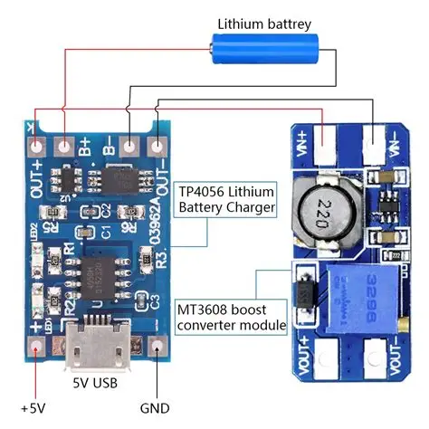
Are you looking for a stable and reliable 18650 battery charging circuit solution for your smart hardware project? Although the market is flooded with various modules, the TP4056 chip remains the top choice for hardware beginners and makers due to its extremely high cost-effectiveness and “foolproof” ease of use. However, ensuring reliable charging and a safe system power supply involves many design details that are easy to get wrong. This article will provide an in-depth breakdown from both an SEO and engineering perspective, covering everything from chip selection, circuit design, and thermal optimization to modern Type-C interface upgrades, helping you build the perfect lithium battery power system.
1. Deep Dive into TP4056 Core Logic: The Three-Stage Charging Algorithm
The TP4056 is not just a simple “5V to 4.2V” step-down module. Its core value lies in its integrated power MOSFET, high-precision voltage reference, current detection, and thermal protection functions, which strictly execute the safe “constant current-constant voltage-trickle” three-stage charging algorithm for lithium batteries:
-
Pre-charge phase: When the battery is in an under-voltage state (below approximately 3.0V), the chip will pre-charge with a very small current (about 10% of the set current) to safely wake up the battery.
-
Constant Current (CC) phase: Once the battery voltage rises above 3.0V, it enters the large-current fast charging phase. The size of the charging current is precisely set by the resistor (Rprog) connected externally to the PROG pin.
-
Constant Voltage (CV) phase: When the battery voltage approaches 4.2V (the standard charge termination voltage for lithium-ion batteries), the chip automatically switches to constant voltage mode. At this time, the voltage is clamped at 4.2V, and the charging current slowly drops as the battery becomes fully charged.
-
Trickle / Termination phase: When the charging current drops to about 1/10 of the set value, the chip determines that charging is basically complete and stops charging; at this point, the STAT pin status changes. If the battery voltage drops below 4.05V due to self-discharge, the chip will restart a trickle charge cycle to maintain a full charge state.
-
Safety Note: The TP4056 strictly follows this physical process, and any design attempting to bypass this process (such as forcibly increasing the termination voltage) sacrifices battery life and safety.
TP4056 Charging State Reference Table (Core Tool for Troubleshooting):
| Charging Phase | Battery Voltage (VBAT) | Charging Current (ICHG) | PROG Pin Voltage | STAT Pin Status (LED Indicator) |
| Pre-charge | < ~3.0V | ~0.1 * I_SET | ~0.1V | Solid ON (Charging) |
| Constant Current | 3.0V ~ 4.2V | I_SET (Constant) | 1.0V | Solid ON (Charging) |
| Constant Voltage | ≈ 4.2V (Constant) | Gradually drops from I_SET | Gradually drops from 1.0V | Solid ON (Charging) |
| Charge Complete | ≈ 4.2V | Near 0 (< 0.1*I_SET) | < 0.1V | OFF (or varies by circuit design) |
| Standby / Battery Power | 4.05V ~ 4.2V | 0 | 0V | Status depends on VCC |
Note: If the battery indicator consistently fails to transition from “Solid ON” to “Complete,” it is highly likely because the set charging current (I_SET) is too small, causing the current to take too long to drop to the termination threshold during the late CV phase.
2. TP4056 Hardware Design Pitfall Guide: 7 Core Practical Points
To successfully translate the datasheet into a stable, working circuit board, the following seven design details will dictate your project’s success or failure:
2.1 Precisely Setting Charging Current: The Science of the PROG Pin Resistor
-
The charging current is configured via the resistor (Rprog) connected from the PROG pin to ground, using the formula:
I_CHG = 1200V / R_PROG. For instance, a 1.2K resistor yields 1A, and a 1.3K resistor yields 923mA. -
Precision Requirements: You must use a 1% precision resistor; using a 5% precision resistor can result in an actual current deviation of up to 20%.
-
Power Dissipation and Packaging: The resistor power calculation formula is
P = I_CHG * 1.0V. When the set current is 1A, the voltage drop across the resistor is 1.0V, meaning the power dissipation is as high as 1W. Therefore, you must select an 0805 or larger package resistor; a standard 0603 package (rated at 1/10W) will instantly overheat or even burn out. -
Thermal Derating Control: The chip features internal thermal feedback, automatically reducing the current when the junction temperature gets too high. In high ambient temperatures or enclosed cases, a set 1A might average only 600-700mA in reality. It is recommended to lower the set value to 500-700mA to enhance system thermal stability and prolong the chip’s lifespan.
# Quick Calculation Example: Setting the charging current to 800mAR_prog = 1200 / 0.8 = 1500 Ohm (1.5KΩ)Resistor Power Dissipation P = 0.8A * 1.0V = 0.8W# Conclusion: You must use a 1206 package resistor rated ≥1W, or use multiple resistors in parallel to distribute the power load.
2.2 Optimizing Input Capacitors to Suppress Power Noise
-
A high-quality ceramic capacitor (typically 10uF) must be placed near the VCC pin; this not only filters noise but also provides transient current at the exact moment charging initiates, preventing the input voltage from dropping.
-
To address resonant oscillations caused by poor-quality power supplies or long USB cables, it is recommended to connect a 1uF X7R or X5R ceramic capacitor in parallel next to the 10uF capacitor to effectively suppress high-frequency noise.
-
Layout Recommendations: The input capacitors should be placed as closely as possible to the chip’s VCC and GND pins, utilizing short and thick traces to prevent operational instability or startup failures.
2.3 Balancing the Voltage Rating of the BAT Pin Capacitor
-
The BAT pin connects to the battery’s positive terminal and typically requires a 4.7uF or 10uF capacitor to stabilize the charging loop and absorb inductive energy when the battery is suddenly disconnected.
-
Voltage Rating Pitfall: The fully charged battery voltage is 4.2V, meaning you must select a capacitor with a rated voltage of at least 6.3V here. If a 4.2V or 5V rated capacitor is used, long-term reliability will be severely compromised.
2.4 Anti-backflow Circuits and External Power Isolation
-
While the chip claims to feature a built-in anti-backflow circuit, this mechanism will fail in complex scenarios where “external power supplies the system and charges the battery when present, and the battery powers the system when absent”.
-
When the external USB 5V is disconnected, the battery voltage of approximately 4.2V will leak backward to the VCC pin through the chip. If the system load is connected to VCC, this creates a uA-level leakage, causing the battery to slowly discharge.
-
Solution: Connecting a low-dropout Schottky diode (like the SS14, which has a voltage drop of about 0.3V) in series on the VCC input path can entirely eliminate this leakage; alternatively, utilizing an ideal diode controller paired with a MOSFET can limit the voltage drop to within a few tens of millivolts.
2.5 Flexibly Using the STAT Pin for Custom UI Indication
-
The STAT pin operates as an open-drain output, conventionally connected to an external LED and a current-limiting resistor tied to VCC (LED ON when charging, OFF when full).
-
UI Upgrade: You can leverage a dual-color LED (common cathode or common anode) combined with a transistor or GPIO to achieve dynamic effects like “red while charging, green when full, flashing on error”.
-
Connecting the STAT pin to an MCU’s GPIO allows the main controller to accurately monitor the charging status, enabling precise charging percentage displays or advanced power management.
// Example: STM32 GPIO reading the charging status (assuming STAT pin low means charging)if (HAL_GPIO_ReadPin(STAT_GPIO_Port, STAT_Pin) == GPIO_PIN_RESET) {// Currently chargingdisplay_charging_animation();} else {// Charging complete or power not connectedupdate_battery_percentage();}
2.6 Cleverly Using PCB Layout to Solve Thermal Design Challenges
-
The primary performance bottleneck of the TP4056 is heat generation, and a well-designed PCB layout serves as the best heatsink.
-
You must enlarge the Exposed Pad (thermal pad) on the bottom of the chip, connect it to a large-area ground copper pour, and stitch it to the ground plane on the back of the PCB using multiple vias to create a three-dimensional heat dissipation channel.
-
Never place temperature-sensitive components, such as temperature sensors or precision reference sources, directly beneath or immediately adjacent to the TP4056.
-
For continuous 1A charging applications, a small physical heatsink can be added, or a window can be opened on the back of the PCB and coated with thermal grease to directly contact a metal enclosure for auxiliary cooling.
2.7 The Indispensable Testing and Validation Phase
-
No-Load Power-On Test: Connect only the 5V power supply; the measured BAT pin should output a stable no-load voltage of around 4.2V, and the STAT pin should read high (LED OFF).
-
Simulated Load Test: Connect a power resistor (e.g., a 4.2Ω/5W resistor for a 1A setting to simulate a battery load); the measured current should closely match the set value, and heat generation should be evaluated.
-
Real Battery Test: Connect a fully depleted 18650 battery, monitor the voltage and current to verify that it completely executes the CC-CV-termination process, and record the total charging duration.
3. Building Smart Power Path Management: Charge-and-Use Seamless Switching
To upgrade a basic charging module into a practical power system that can “charge and be used simultaneously” and switch seamlessly when external power is unplugged, an external circuit must be implemented; the most reliable method is using a P-MOSFET.
3.1 P-MOSFET Switching Circuit Working Principle
Taking the AO3407 (P-MOS) as an example, it effectively forms an automatic "power selector":
External Power (5V_USB) ------> TP4056.VCC|| (Optional diode, for anti-backflow and step-down)VSystem Load (VCC_SYS)^|Battery Positive (BAT+) ------>|--(Source S) P-MOS (AO3407) (Drain D)--||Gate G connects to 5V_USB
-
When 5V_USB is Plugged In: The external power supplies the system and also connects to the MOSFET gate (G). Because the gate voltage is higher than the source voltage (battery voltage approx. 4.2V) minus the threshold voltage, the P-MOSFET turns off. The path between the battery and the system is severed, meaning the battery only accepts a charge, achieving a physically isolated and safe “charge-and-use” environment.
-
When 5V_USB is Unplugged: The gate is pulled to a 0V ground level by a pull-down resistor (typically 100K). Because the gate voltage is far lower than the source voltage, the P-MOSFET turns on. The battery voltage flows to the system power supply through an extremely low on-resistance. This transition is completely automatic and seamless, and the voltage drop loss is far lower than that of a Schottky diode (0.3V), drastically improving energy utilization efficiency.
3.2 MOSFET and Component Selection Calculations
-
Vgs(th) Gate Threshold Voltage: You must ensure that when 5V_USB is connected (Vgs = 5V – VBAT ≈ 0.8V), the voltage is high enough to reliably turn off the MOSFET. It is recommended to select a model with an absolute threshold voltage between -1V and -2V.
-
Continuous Drain Current (Id): This parameter must exceed the maximum operating current of the system.
-
On-Resistance Rds(on): The smaller this parameter is, the better, in order to minimize heat generation and voltage drop. The AO3407 features an on-resistance of about 40 milliohms at Vgs=-4.5V, resulting in only a 40mV voltage drop and 40mW power dissipation when passing 1A of current, which is exceptional.
-
Gate Pull-down Resistor: The resistance is generally chosen to be between 10K and 100K. A value that is too large makes the circuit susceptible to interference, while a value that is too small leads to unnecessary power waste when external power is plugged in.
4. Embracing the Modern Type-C Interface Upgrade
Micro-USB is rapidly being phased out, and adopting Type-C not only eliminates the frustration of plugging cables in backward but also massively enhances power compatibility.
4.1 Basic “Charge-Only” Upgrade Solution
-
If your application only requires the Type-C port to provide 5V power without needing data functionality, you merely need to configure a Type-C receptacle with CC pull-down resistors.
-
Connect a 5.1KΩ (1% precision) resistor to ground on either of the two CC (Configuration Channel) pins (though connecting both is highly recommended).
-
Connect VBus in parallel to the TP4056’s VCC, and tie GND in parallel to the system GND.
-
With this setup, any standard Type-C power supply (including both C-to-C and A-to-C cables) will recognize that the device requires 5V power and will activate its output.
4.2 Advanced Upgrade: Supporting USB PD 5V Protocol
-
Some modern power banks or chargers default to not outputting 5V on their Type-C ports; in this scenario, an inexpensive USB PD protocol chip (such as the IP2723T or CH224K) can be added to handle the handshake.
-
The protocol chip negotiates via the CC line to request a fixed 5V output, and uses a “protocol enable” signal to control a MOSFET to connect VBus, thereby achieving much broader power compatibility assurance.
4.3 Physical Layout and ESD Protection
-
Large Current Carrying Capacity: The Type-C interface contains multiple VBus pins, so you must connect A4, B4, A9, and B9 all together using thick copper traces inside the PCB to ensure the port can safely carry a maximum of 3A current.
-
Electrostatic Surge Protection: You must place a Transient Voltage Suppressor (TVS, such as the SMBJ5.0A) diode at the VBus input to block static electricity or high voltage spikes caused by plugging/unplugging from damaging the downstream TP4056.
-
Interface Reinforcement: Select a Type-C receptacle equipped with a metal shell and positioning pegs, paired with robust PCB mounting pads, to prevent the interface from becoming loose during daily plugging and unplugging operations.
Conclusion: By integrating a Type-C input, TVS protection, the core TP4056 charging circuit, and P-MOSFET-based power path management, this complete 18650 battery power supply solution remains low-cost yet thoroughly engineered, making it fully capable of serving as the core foundation for serious smart hardware prototype development.